Part 3. Procedure
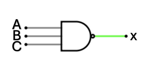
| A | B | C | x |
|---|---|---|---|
| 0 | 0 | 0 | |
| +5 | 0 | 0 | |
| 0 | +5 | 0 | |
| +5 | +5 | 0 | |
| 0 | 0 | +5 | |
| +5 | 0 | +5 | |
| 0 | +5 | +5 | |
| +5 | +5 | +5 |
| A | x |
|---|---|
| 0 V dc | |
| +5 V dc |
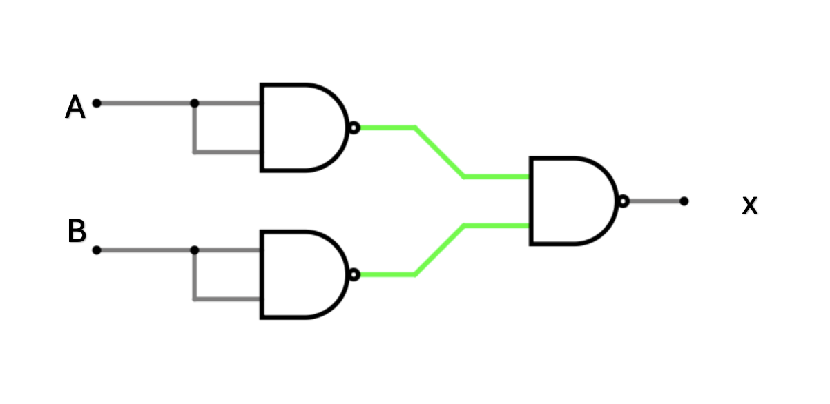
| A | B | Output |
|---|---|---|
| 0 | 0 | |
| 0 | +5 | |
| +5 | 0 | |
| +5 | +5 |
| A | B | x |
|---|---|---|
| 0 | 0 | |
| 0 | +5 | |
| +5 | 0 | |
| +5 | +5 |
| A | B | C | x |
|---|---|---|---|
| 0 | 0 | 0 | |
| +5 | 0 | 0 | |
| 0 | +5 | 0 | |
| +5 | +5 | 0 | |
| 0 | 0 | +5 | |
| +5 | 0 | +5 | |
| 0 | +5 | +5 | |
| +5 | +5 | +5 |
| A | x |
|---|---|
| 0 V dc | |
| +5 V dc |
| A | B | Output |
|---|---|---|
| 0 | 0 | |
| 0 | +5 | |
| +5 | 0 | |
| +5 | +5 |
| A | B | x |
|---|---|---|
| 0 | 0 | |
| 0 | +5 | |
| +5 | 0 | |
| +5 | +5 |